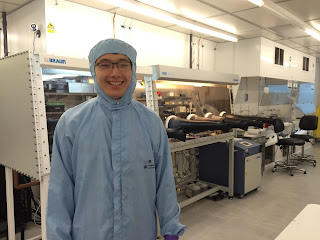
 Michael Collis recently completed his SATROclub Extended Research Placement at the University of Surrey under supervision of Dr Radu Sporea. Michael was tasked with investigating next-generation electronic circuit applications made on large areas with unconventional technologies such as inkjet printing and resulting in flexible, low-cost and power efficient electronics.
Here's what Michael had to say about his time at the University...
Week One:
This week I have been learning all about transistors, and
preparing for the lab work that I will be doing during the next few weeks.
First, I read part of “Electronics for Today and Tomorrow” by Tom Duncan,
particularly the sections on semiconductors, diodes and transistors. I learnt
the differences between n-type and p-type semiconductors (the former has
electrons as charge carriers, the latter has positive “holes” as charge
carriers), as well as about the junction that is created between the two when
they are placed together. I then went on to learn about the junction transistor,
which is the less common, but simpler type of transistor often used in high
current applications, followed by the junction field effect transistor, and how
they work. With this base understanding, I then learnt about
Metal-Oxide-Semiconductor Field-Effect-transistors, otherwise known as the
MOSFET, the most common of transistors today, used all the time in integrated
circuits, which is very close to what my project is on. I went into more detail
in these, also learning about its’ electronic characteristics and equations to
model it, as well as how and where they are used. Finally, I applied this
knowledge to the source-gated transistor, which my project is on. At this
stage, I also learnt about possible production techniques, as well as the
theory behind using an inkjet printer to create them. Finally, I made a general
plan of the next three weeks with Dr Sporea, so that we can make the most out
of the time available.
Week Two:
This week started with safety talks, first for the general
labs, then for the clean room. I also obtained my amazing blue clean room suit.
The first two days were getting used to the inkjet printer, which I printed a
protective layer on copper covered plastic in certain designs (starting simple,
but getter more complex on Tuesday). On
Tuesday morning, I met Professor John M Shannon, the person who discovered and
wrote the first paper on the Source Gated Transistor. On Wednesday, I etched my
previously made designs in the copper in the clean room, before attempting to
print silver electrodes on glass. I spent the whole day on Thursday in the
clean room, preparing substrates, coating them in different substances and
using masks, using the JLS Sputterer and other pieces of equipment, as well as
making a semiconductor solution. During which, I made metal electrodes on
glass, followed by a dielectric and them more metal, putting via holes in some
of them, to test Via holes. On Friday I measured the current and resistance of
the samples from Thursday, which gave out good results. Afterwards, I attempted
to print a semiconductor ink, which failed due to clogging, before reading
through numerous papers on Via hole printing so that we can try and improve our
process.
Week Three:
This week I started by cutting around 30 glass substrates,
for creating source gated transistors on. Before I could do this, I had to
clean all the glass by first blowing each substrate with high pressure nitrogen
gas, to get rid of any dust particles. Then, I placed them in beakers filled
with acetone, and placed the beakers in a agitated water bath for five minutes.
Next, I took them out of the water bath and rinsed them with acetone, before
blow drying them with nitrogen gas. I then placed them in another beaker filled
with isopropanol and then in the agitated water bath for 5 minutes. I rinsed
the samples with isopropanol and blow dried with nitrogen gas. Finally, I
placed them in a machine that fired high energy oxygen ions at the substrate,
finally giving us a atomically clean substrate. Afterwards, I used the JLS
sputter machine to place source and drain electrodes on the substrates, using
different metals. Then I deposited two different semiconductors, insulator and
finally a gate on the substrates. On Friday, I finally got to measure the
electrical characteristics of the transistors; even though most had short
circuits, the one that worked showed great electronic characteristics.
No comments:
Post a Comment